Introduction
By utilizing the make cscope to create cscope database, I could browse a
specific build without being confused by a lot of symbols with same names.
This document describe very basic scenario on how to read the u-boot source
code.
start.S
After loading the cscope.out, I could find search the starting point by the following command
cs find f start.S
This leads me to the file arm/cpu/arm1136/start.S.
SVC32
SVC32 mode is the mode with highest privilege.
reset:
	/*
	 * set the cpu to SVC32 mode
	 */
	mrs	r0,cpsr
	bic	r0,r0,#0x1f
	orr	r0,r0,#0xd3
	msr	cpsr,r0
From the ARM11 specification, http://infocenter.arm.com/help/topic/com.arm.doc.ddi0360f/DDI0360F_arm11_mpcore_r2p0_trm.pdf, Section 2.9, we could learn that the register CPSR’s bit 0 to bit 4 contains the processor operating mode.
In Section 2.9.7, we learned that value b10011 will set the processor to
supervisor mode.
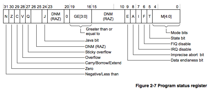
bic (bit clear) clears the r0’s bit 0 to bit 4. And orr instruction sets
the bit 0b11010011, apart from setting the mode to SVC mode, it also disables
FIQ and IRQ.
flash caches
cpu_init_crit:
/*
* flush v4 I/D caches
*/
mov r0, #0
mcr p15, 0, r0, c7, c7, 0 /* Invalidate I+D+BTB caches */
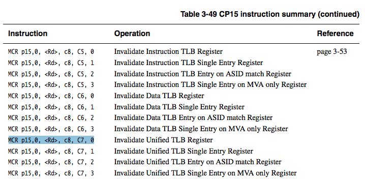
mcr p15, 0, r0, c8, c7, 0 /* Invalidate Unified TLB */
The first instruction about “Invalidate I+D+BTB caches” could be understood
from the following figure in “ARM11 MPCore™ Processor Revision: r2p0 Technical
Reference Manual”: 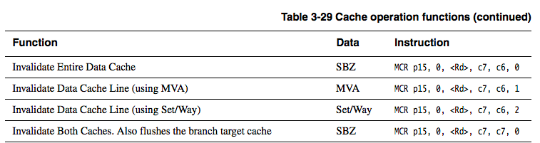
The instruction about TLB could be understood from following figure:
disable MMU and data cache
	/*
	 * disable MMU stuff and caches
	 */
	mrc	p15, 0, r0, c1, c0, 0
	bic	r0, r0, #0x00002300	@ clear bits 13, 9:8 (--V- --RS)
	bic	r0, r0, #0x00000087	@ clear bits 7, 2:0 (B--- -CAM)
	orr	r0, r0, #0x00000002	@ set bit 1 (A) Align
	orr	r0, r0, #0x00001000	@ set bit 12 (I) I-Cache
	mcr	p15, 0, r0, c1, c0, 0
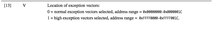
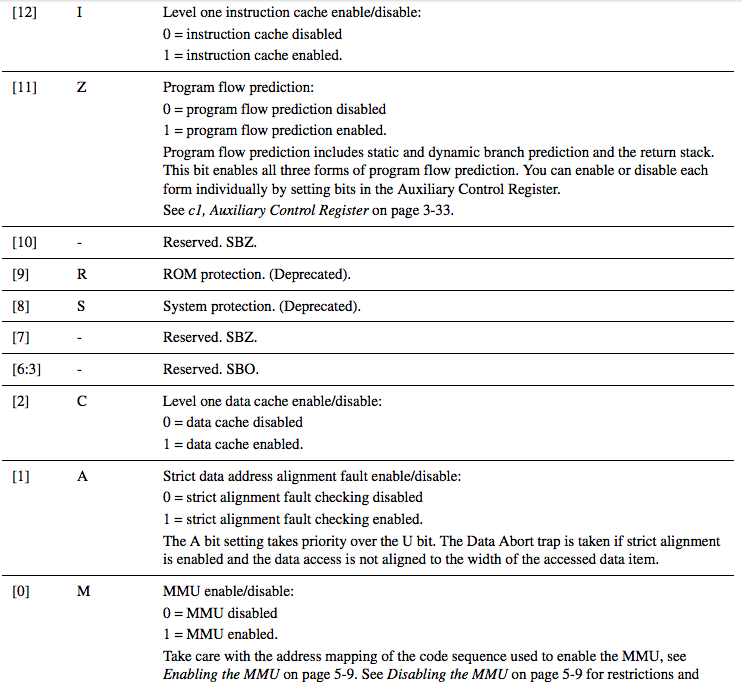
According to following figure:

The code first reads the control register to r0, then modifies the value of
r0 and writes it back to control register.
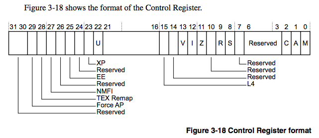
Detailed description are in following figures. The code first clears following bits:
- bit 13, which selects the low normal exception vectors which range is address range = 0x00000000-0x0000001C.
- bits 9:8 is the ROM protection and System protection.
- bit 7 is “Reserved”, I am not sure why the code needs to clear the bit.
- bit 2:0 which is C , data cache disabled; A, strict alignment fault checking disabled; M, MMU disabled.
The code set following bits:
- bit 1: strict alignment fault checking enabled
- bit 12: instruction cache enabled
The instruction cache is enabled in the code which looks not aligned with the comments “instruction cache enabled”.
Continue with part 2